Xiaomi Zigbee (1): Getting to know the hardware
*
Preface
Xiaomi is a rising player in the field of IoT devices. They offer everything from smart bulbs, through smart rice cookers, to smart robot vacuums - and its range of smart home devices is constantly growing. While some of their devices use WiFi for communication purposes, others use ZigBee - a low-power, wireless mesh network protocol.
Prior research of the Xiaomi ecosystem has mostly focused on their WiFi-based devices. Therefore, we chose the ZigBee-based devices as the focus of this research.
Xiaomi’s ZigBee based ecosystem contains a multitude of different devices:
- Light bulbs
- Power plugs
- Wired/wireless switches
- Presence sensors
- Door/window contact sensors
- Temperature/humidity/vibration/pressure sensors
- Water leak sensors
- Smoke detectors
- Smart locks
- Curtain motors
While the WiFi-based devices can work autonomously, all of the above devices need a ZigBee gateway. The gateway is connected to the internet, and exposes the ZigBee devices to Xiaomi’s MiHome apps.
We chose Xiaomi’s smart power plug (model ZNCZ02LM) as the first device for this research. This series of posts documents the process of reversing the plug’s hardware, as well as preparing the reverse engineering infrastructure required for vulnerability assessment of its firmware.
Xiaomi Smart Plug (ZNCZ02LM)
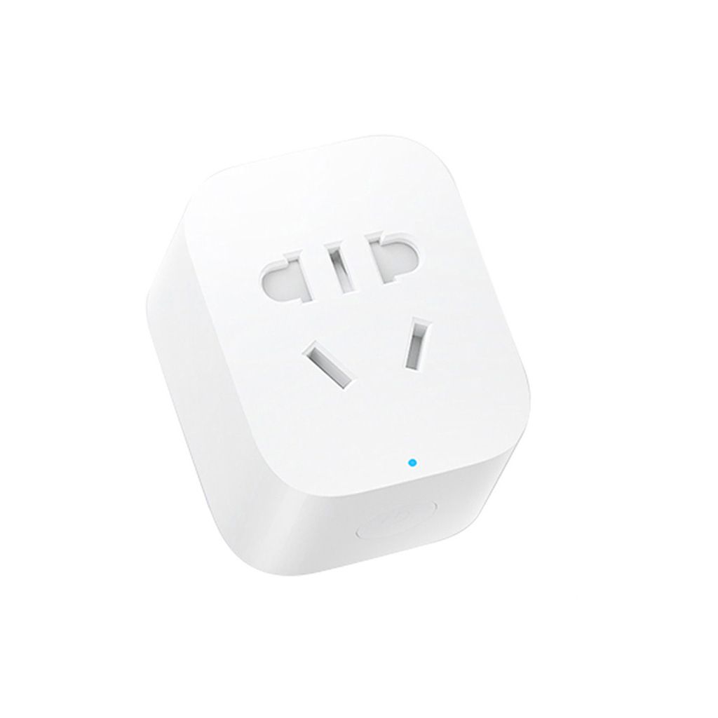
The smart plug can be used to turn a regular mains socket into a smart one. It can be turned on and off either via a physical button, or via the MiHome app. A blue LED light indicates whether the plug currently provides power. Furthermore, the plug monitors current flow, and information about electricity usage is available in the MiHome app.
A look inside
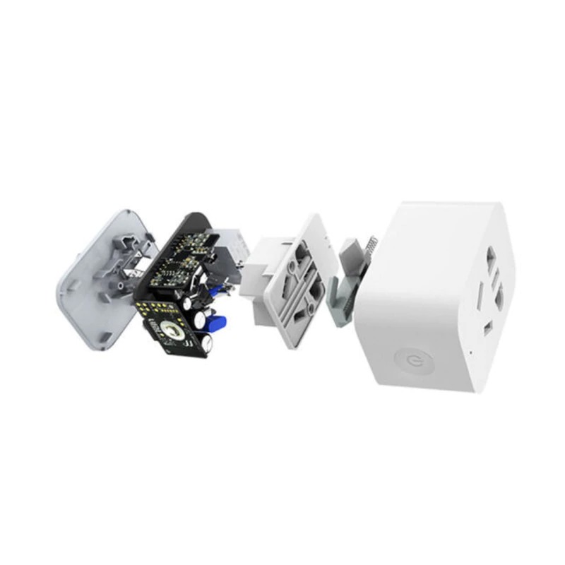 Exploded View (Illustration)
Taking the plug apart requires a spudger or a flat screwdriver, and cosmetic damage seems inevitable. Opening it reveals a big board with the mains electrical connectors, several capacitors, a relay, and 2 additional boards. One of the smaller boards seems to be responsible for measuring the power (power consumption measurement is one of the advertised features), while the other houses the actual MCU. The boards are all marked LUMI - the actual manufacturer.
 MCU Board - Top Side
 MCU Board - Bottom Side
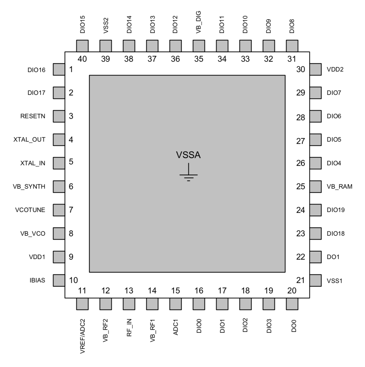
The board of interest for us was the MCU board. It includes the MCU itself - the smart component that we will attempt to attack - and a bunch of pinouts that look like they could be used for debugging, and whatnot. Lucky for us, it could be easily disconnected from the main board, allowing a much easier inspection. A closer look at the MCU revealed its model: JN5169. This is a Jennic (now NXP) ZigBee MCU, with a custom architecture (the research of which will be covered in another post).
Armed with the knowledge of the MCU’s model, we used the powers of the internet to hunt down its datasheet and other documents provided by NXP. These documents allowed us to identify the chip’s pinout, and know the purpose of each of the pins. Of special interest were pins responsible for power (for powering the board independently), UART (for communicating with the board), and JTAG (for debugging).
Hooking the board up
Lucky for us, the board has many test points. Once we found the relevant pins, we could attempt to trace them to the test points. Connecting to the test points is a lot easier than connecting directly to the chip itself.
In order to hook the board up for research, we needed information about the following pins of the MCU:
- Power:
VDD(positive voltage) andVSS(ground) - UART:
RXandTX(CTSandRTSare not needed, in our case) - JTAG:
TCK,TMS,TDO, andTDI
The pin configuration/assignments of the 40-pin QFN JN516X chip can be found in the datasheet from NXP (JN-DS-JN516X), pp. 9-11.
By tracing the various test points and jumpers on the board to the MCU, we came up with the following connection matrix:
| JN5169 | JP1 | JP2 | Test Point | Function |
|---|---|---|---|---|
| 28 | 1 | TXD0 | ||
| 29 | 2 | RXD0 | ||
| 22 | 3 | SPIMISO | ||
| 9/30 | 4 | 8 | TP30 | VDD |
| 3 | 5 | RESETN | ||
| 21/39 | 6 | 1 | TP29 | VSS |
| 26 | 2 | TP16 | PC0 (?) | |
| 27 | 3 | TP15 | PC1 (?) | |
| 17 | 4 | TP19 | PC0 (?) | |
| 31 | 5 | TP17 | PC1 (?) | |
| 19 | 6 | TP18 | RFTX (?) |
In the above table, JP2 pins (see the 8-pin connector on the bottom side of the MCU board) are counted from left to right, from top to bottom (when looking at the connector from the top, reading the JP2 label correctly). JP1 pins (see the 6 pins labeled JP1 to the left of the switch button on the top of the MCU board) are counted from the top (with pin 1 being next to the triangle marker). The test points can be found on the top side of the MCU board, next to the JP1 pins.
Surprisingly, TP25 and JP2[7] were not traced to any pin on the MCU.
Power
We easily identified the power pins and the required voltage (3v3). VDD was traced to TP30, while VSS was traced to TP29.
UART
The MCU has 2 UARTs - UART0 (TXD0/RXD0) and UART1 (TXD1/RXD1). UART0 can be mapped either to pins 28-29, or to pins 38, 40. UART1 can only be mapped to pins 38, 40. Tracing these pins to the different testpoints revealed that JP1[1] is TXD0, and JP1[2] is RXD0.
JTAG
JTAG on the JN516X is enabled by the MCU during the boot sequence, based on the CPU_JTAG bit in the index sector (a special, one-time programmable area of the embedded flash used for secure storage of customer settings; see JN-AN-1003, p. 12) and the “Software Configuration Options” of the booting firmware (part of the firmware header responsible for JTAG configuration; JN-AN-1003, p. 19). Disabling the JTAG via either of these flags is sufficient. As we will see later in firmware analysis, JTAG support is disabled in the Software Configuration Options, preventing JTAG debugging of the MCU.
Exploring the serial interface
Regular UART
Intrigued by the MCU’s serial interface, we hooked up the UART testpoints to our computer. We powered the board with a 3v3 power supply, and used buadrate.py to identify the correct baudrate for the connection. It’s a nifty little utility that changes the serial connection’s baudrate on the fly, while piping the output to the screen. When the correct baudrate is selected, the output becomes readable (this, of course, assumes that the serial output is textual in its nature).
Luckily, the output was textual, and available at a baudrate of 115200. Following is a sample UART output, captured during the board’s boot:
APP: Light Power Up = 2

=======================================================================
=             (C) COPYRIGHT 2016 Lumi Tech                            =
=                                                                     =
=                   System infomation                                 =
=                                                                     =
=                   APP_VERSION--> V1.3.22                            =
=                   ModelID--> lumi.plug                              =
=          Fireware BuildTime: 02-28-2017 16:58:51                    =
=                                           By Lumi tech  Team        =
=======================================================================

sizeof(tsFactoryParam) = 32
sFactoryParam.u8FactoryTestOK = 1
sFactoryParam.u16RelayOffDelay = 4500
sFactoryParam.u16RelayOffDelay = 5500
sFactoryParam.u16PowerSlope = 460
sFactoryParam.i16PowerOffset = 0
sFactoryParam.u16VoltageSlope = 35
sFactoryParam.i16TempOffset = -9
sFactoryParam.bProtectEnable = 1
sFactoryParam.u8ProtectPower100w = 25
sFactoryParam.u8ProtectTempC = 70
sFactoryParam.u8HardwareVersion = 19
sizeof(te_LumiNVMData_t) = 64
LumiNVMData.u8PrevOtaVersion: 0
u8SegDataLen= 64 , sizeof(tsLBT_MapsStorage)= 2856
PDM read bytes = 2856
eStatusLBTReload=0
sDeviceDesc.eNodeState  = E_STARTUP
Radio Channel--> 0
PAN Id--> 0x0
EPAN Id--> 0x0000000000000000
Short Network Id--> 0xffff
IEEE Addr Id--> 0x00158d00022db526

NT Size: 26 u8NTNum 0 u8ChildNum 0
AvailbeNTSize--> 0x0000

APP_ZCL_vInitialise Finished

App_Initialise Finished

OS started


APP: APP_ReportTelegrame Task--> bOnOff:0  TriggerSource:2
APP_ReportTelegrame_Task--> 2000-01-01  00:00:06 Sunday
At this point, pressing the button on the MCU board would trigger additional lines (similar to the last 2 lines above), switching the plug on and off, as expected.
Unfortunately, this UART interface seems to be used for logging only, as writing to it would not yield any results. Still, it produces some interesting data that might be useful when analyzing the firmware - mainly, variable names and their values.
Bootloader UART
While the regular firmware UART’s functionality is lacking, it’s not the end of the world. The MCU’s bootloader supports serial communications as well (unless its Code Readout Protection, a security mechanism that prevents reading the embedded flash from external (UART/JTAG) interfaces, is at level 2; see JN-AN-1003, p. 12). In order to get the MCU into the bootloader serial interface, the SPI MISO pin has to be held low during boot (see JN-AN-1003, p. 1).
Looking up the pin configuration, we saw that SPI MISO is mapped to pin 22, and traced to JP1[3]. Powering up the board with the test point connected to ground, we connected to the bootloader’s serial interface. This was considerably more interesting than the firmware one, as it is interactive!
The serial protocol is documented in detail on pp. 24-30 of JN-AN-1003. It uses baudrate 38400 initially (though this can be increased once communication is established). Several tools implementing this protocol are available, both in C and in Python:
- jenprog: A Jennic bootloader programmer in Python, by Philipp M. Scholl
- JennicModuleProgrammer: A Jennic bootloader programmer in C
- zigbee-flasher: A newer version of JennicModuleProgrammer, above.
The bootloader protocol supports various commands for reading, writing, and executing the MCU’s flash memory and RAM. This could potentially be used for fetching the firmware for further analysis.
Unfortunately, our progress in this direction was stalled by CRP (Code Readout Protection). This is a mechanism for preventing unauthorized access to the flash of the MCU. The CRP on our production board is set to level 1 (this was evident by our failed attempts to write values to RAM, and validated by reading the CRP value from the device’s memory). At this level, several functions of the bootloader are disabled (see JN-AN-1003, pp. 25-27). Specifically, we couldn’t issue Flash read requests (message type 0x0B), RAM write requests (message type 0x1D), and Run requests (message type 0x21). This prevented 2 basic approaches to extracting the firmware:
- Directly reading the flash via Flash read request
- Uploading a piece of code to RAM and executing it (the code would read the flash and output the read values via UART)
We fuzzed the serial interface with every possible message type, hoping to hit an undocumented functionality. The following code depends on jenprog, and assumes that the response message type is always the request message type plus 1. It can be easily rewritten to access the serial interface directly via pySerial, and accept any message type in response (though doing so did not yield any additional undocumented message types).
#!/usr/bin/env python

import con_serial

def main():
    bl = con_serial.SerialBootloader('/dev/cu.usbserial-TIM02108B', select_flash=True)

    for byte in range(0x99):
        print(byte, '-'.join([str.format("{:02x}", i) for i in bl.talk(byte, byte + 1)]))
        print(byte, '-'.join([str.format("{:02x}", i) for i in bl.talk(byte, byte + 1, data=[byte]*byte)]))

if __name__ == "__main__":
    main()
We did, in fact, find an undocumented message type, 0x68, that returned data (every other invalid message type returned the same response). However, the responses didn’t prove valuable, and couldn’t be used to advance us towards firmware extraction.
We considered downgrading CRP to level 0 (unsecure) by overwriting the index sector. The sector is memory mapped to a known address in RAM (0x01001000). However, writing to that RAM address (in the hope that it’ll be passed through to flash) is impossible with CRP at level 1. Furthermore, by reading the code of zigbee-flasher, it’s clear that writing the index sector is not a simple matter (zigbee-flasher actually loads an extension into the device’s RAM, and then executes it in order to write the sector - again, impossible with CRP at level 1). Given the complexity of the task, and the low chance of success (after all, the sector is supposed to be read-only after the initial programming at the factory), this idea was abandoned.
Getting the firmware
Finally, we decided to try and use the gateway, in the hope that a firmware update will be downloaded for the device, and we will be able to sniff it over the network. Upon setting everything up (the gateway, the MiHome app, and sniffers at various points), it was time to connect the plug to the gateway, and hope for an update. Unfortunately, due to a mistake in the setup, we missed the download of the plug firmware (instead only capturing the firmware for the gateway itself).
As we were about to turn our attention to the gateway (after all, we had its firmware in hand), we stumbled upon a firmware for the Xiaomi plug, captured or extracted by another team researching Xiaomi devices (mentioned above). Ironically, it was the version of the firmware that came with our smart plug, prior to it being updated by the gateway.
What’s next?
Now that the firmware was in our hands (thanks to the talented team behind the Xiaomi Robot Vacuum research), it was time to reverse it - but before we could do that, we needed to get acquainted with the MCU’s architecture. Join us in the next post, as we discuss the development of a disassembly and analysis plugin for radare2, targeting JN516X!